Lab of the fun QSIM Functional Quantum Spin-Iontronic Materials
|
Modern technology has
evolved to a stage that careful manipulation of a single spin or charge
carrier is no longer a formidable task. Our research focuses on a
particular aspect of the electrons - their spin degrees of freedom, and
spin information can be stored, transferred, and processed all the way
from classical to quantum levels.
We can efficiently harvest the mutual interactions between spins
and ions in nanoelectronic devices (ie, spin-iontronics) for advanced spin control and monitoring. The freedom
to combine complex spin systems, ion systems, topological states, and
superconductors grants us the unique advantage in bottom-up materials
design and construction, while still keeping
mass production and integration in check. Our program has a strong
emphasis on the development of novel materials and devices towards more
powerful yet more energy efficient information processing units, into an
era beyond silicon. Research
Interests: * Topological
quantum computing on low-dimensional spin systems * Spin memory
and logic devices * Superconducting
microwave circuits * Spiontronics for Field
Programmable Neural network Arrays (FPNA) * RRAM for
Compute in Memory architectures Funding: >
Ontario Early
Researcher Awards >
Canada First
Research Excellence Fund - Transformative
Quantum Technologies >
NSERC,
Discovery, Engage >
Mitacs, Accelerate >
ECE department
research stimulation grant Courses taught: (please log in to your LEARN account to access the
course notes and updates) •
NE226 “Characterization
of Materials” •
ECE231 “Semiconductor
Physics and Devices” •
NE353 “ Nano Probing and Lithography” •
ECE403 “Thermodynamics” •
ECE405D “Superconducting
Quantum Circuits” •
NANO600 “Introduction
to Nanotechnology” •
NANO601 “Characterization
of Nanomaterials” •
ECE630 “Physics and
Models of Semiconductor Devices” •
NANO701 “Solid State
Physics and Chemistry” •
NANO702 “Nanoscale
Phenomena” •
ECE730-T19 “Magnetism
and Spintronics”
|
A tiny diamond ring (400 nm OD, 100 nm width)
A picture
carved into diamond (20 μm x 20 μm) |
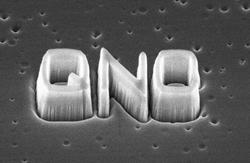
(100
nm line width)
Array
of diamond nano-pillars (100 nm diameter) |
||||||||
|
(100 nm line width)
Angle-resolved
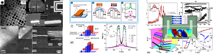
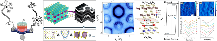
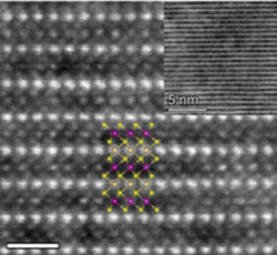
photoemission spectroscopy (ARPES) mapping on 2x2 Mn intercalated TaS2
at Canadian Light Source (CLS) synchrotron beam line, clearly revealing
the existence of a flatband across the whole
k-space |
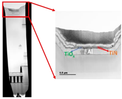
Back-end-of-line (BEOL) integration of battery-like,
reconfigurable memristors on TSMC CMOS chips Mn intercalated transition-metal dichalcogenide (TMD) TaS2 |
|||||||||
|
|
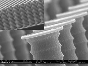
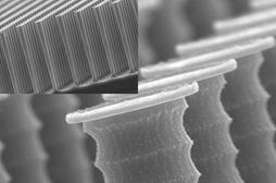
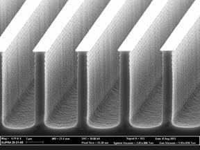
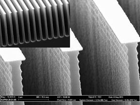
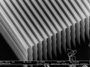
Anisotropic dry etching on Si Anisotropic wet etching on Si mask
diameter 1.5 µm, pillar depth 17 µm mask width 300 nm, trench depth 2 µm mask width 2 µm, spacing 2 µm mask width 1.5 µm, depth 13 µm |
|
|
|||||||
|
|
||||||||||
|
|
|
|||||||||