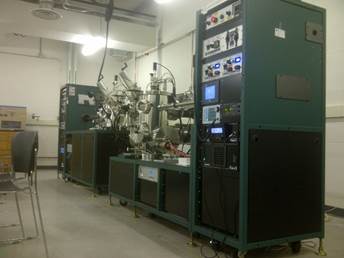
Sputter/Evaporation Dual Chamber System (AJA Orion)
Commissioned in Feb. 2013
|
|
|
The system is designed for 3-inch
wafers, with substrate rotation 0-40 rpm and heating up to 850°C. System base
pressure is better than 1×10⁻⁸ torr. The magnetron sputter chamber
is equipped with 10 sputter guns, and RHEED growth monitoring. The
evaporation chamber is equipped with one e-gun (5-pocket, 5kW) and four
thermal sources, plus an atomic gas source for the reactive growth of oxides
and nitrides. An additional wafer handler enables substrate tilting during
evaporation. The load-lock chamber is equipped with a 6-cassette shadow mask
changing system. |
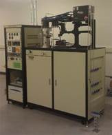
Diamond CVD (SEKI AX5250M)
Commissioned in June 2012
|
|
The AX5250 microwave plasma
reactor incorporates 5 kW at 2.45 GHz microwave generator to produce plasmas
at high power densities. Such operation allows a new regime of plasma
chemistries. This reactor at our facility is dedicated to synthesizing high
quality single crystal and poly crystalline diamond. Light doping, e.g., with
Nitrogen, is facilitated with the natural presence of impurities in the
processing gases, while heavy doping, e.g. with Boron/Phosphorus, is achieved
by introducing additional gas channels. The system can accommodate up to
three dopant gases. The maximum wafer size 2”, and the maximum processing
temperature 1100°C. |
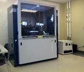
XRD (Bruker D8 Discover)
Commissioned in May 2013
|
|
This X-ray analyzer is capable of
performing high-resolution X-ray diffraction, gracing incidence diffraction,
reflectometry, and reciprocal space mapping. It consists of a centric Euclerian cradle with Chi/Phi rotations and X-Y-Z
translations; high resolution optics with a Ge 2-bounce monochromator, a
3-bounce pathfinder, and fully automated slits; a Göbel mirror for Cu
radiation. The system is equipped with a vacuum chuck holding up to 5”
wafers. |
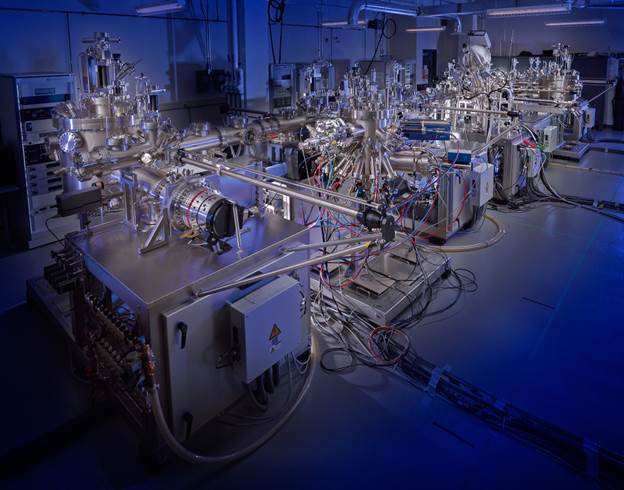
UHV Cluster Deposition System
(Omicron)
(commissioned in Dec. 2014)
|
|
|
This large scale thin film
deposition system has three Molecular Beam Epitaxy (MBE) systems, two
magnetron sputter systems, and one surface analysis module, all
interconnected through a linear transfer line. This system is uniquely
designed to combine the three major spin systems, magnetism,
superconductivity, and quantum spin Hall state, completely in situ under ultra-high vacuum and
maintain the cleanest interfaces possible. The three MBEs are dedicated to
perovskite oxides (YBaCuO, SrTiO,
LaSrMnO, etc.), metal / ferrites (XFe2O4)
/ binary compounds (MgB2 etc.), and topological insulators (Bi/Te/Se with Cu/Ca/Cr doping), respectively. The metal MBE
chamber is equipped with an additional 6-cell linear e-gun. The two sputter
systems are devoted to depositing more conventional magnetic materials (12
guns) and superconductors (8 guns), respectively. The analysis module enables
sensitive surface characterizations with XPS (X-ray photoelectron
spectroscopy) / AES (Auger electron spectroscopy) / UPS (ultra-violet photoelectron
spectroscopy), and is equipped with an ion sputter gun for depth
profiling. A sample preparation
sub-chamber, located right next to the load-lock, allows for well controlled
device surface treatment before, after, or in between film growths
(annealing, ion milling, oxidation / nitridation, etc.). Shadow mask assembly
is available in the load-lock, substrate tilting in the metal MBE, atomic gas
sources in both oxide and metal MBEs, and RHEED in all three MBEs. The system
base pressure is 1×10⁻¹⁰ torr for MBE / surface analysis, and 1×10⁻⁹
torr for sputtering. The standard wafer size is 2”. Maximum substrate
temperature is 1100°C in the MBE systems, 850°C in the sputter systems, and
527°C in the analysis module. The system has detachable vacuum transfer
shuttles for transporting delicate specimen, while maintaining under UHV,
into other growth/characterization systems, for example, to the ALD (atomic
layer deposition) / PECVD (plasma enhanced chemical vapor deposition)
deposition systems (located at QNC on campus) for the growth of high quality
dielectrics and semiconductors, or to the Canadian Light Source beam lines
for advanced ARPES analysis (Angle-resolved photoemission spectroscopy). |